C band low noise amplifier theory Circuit Diagram But there is more to designing low noise circuits than choosing the lowest voltage noise density (e n) amplifier for a given frequency band. As shown in Figure 2, other noise sources come into play, with incoherent sources combining as a root sum of squares. Figure 2: Op Amp Circuit Noise Sources First, consider resistors as noise sources.

On the other hand, someone into radio astronomy definitely requires a very low noise amplifier to receive the hydrogen line frequency emanating from the milky way. In this blog post, I show how I designed a low-noise amplifier having bias-tee for power delivery through coaxial cable and an arrangement for bandpass filter. The specifications Low-Noise Amplifiers Design Specs • Noise Figure: requires very low noise in the input device. For a simple CS stage, the transistor gm must exceed 1/(25 ohms) if the noise figure is to remain below 2 dB. Exercise: calculate the NF if the metal line connecting to the gate has a resistance of Rm. Æ Only one device should dominate NF.

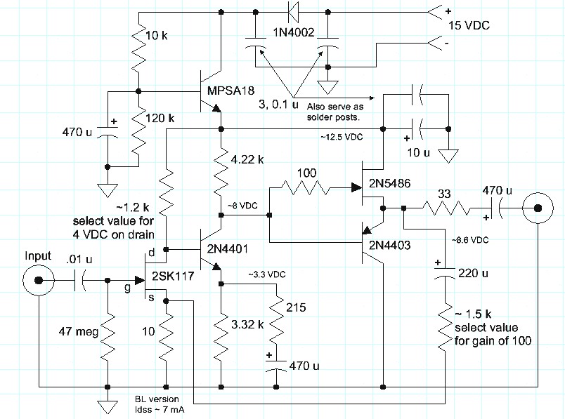
Low noise amplifier design Circuit Diagram
Low Noise Amplifier Design and Optimization IV.1 CMOS LNA Design and Optimization Overview Low Noise Amplifier (LNA) is the most critical part of a receiver front end, in term of the receiver performance. Many circuits with different configurations have been proposed for LNA, in different applications.

R 1 and C 3 form a simple feedback circuit that helps regulate the operating voltage on C 3. The input voltage, Use the Biased for LNA in your template file as a starting design. The design of the low noise amplifier is explained in the following videos. The basic steps for design are as follows: cularly valuable because any low frequency or burst noise can be observed. If the pre amp does not dominate the noise generated from succeeding stages (with the gain control at a maximum) then these stages need to be examined! The full design of a general-purpose au dio preamplifier can be quite a problem,
PDF Designing with Op Amps for Low Noise Circuit Diagram
Designing a Low-Noise Amplifier demands a systematic approach, integrating theoretical principles with practical implementation. Leveraging Advanced Design System (ADS), designers can navigate the intricate intricacies of LNA design, from defining specifications to fabricating and testing the finalized circuit.